If you’ve worked with rigid-flex PCBs long enough—whether as an engineer, a product designer, or a procurement lead—you know they’re the unsung heroes of modern electronics. They combine the structural stability of rigid PCB layers with the flexibility of thin, bendable polyimide (PI) or polyester (PET) films, making them perfect for everything from wearables and medical devices to aerospace components. But here’s the thing: rigid-flex PCBs are also notoriously prone to unique defects that can derail even the most well-planned projects. Over the past 12 years, I’ve been a rigid-flex PCB supplier, and I’ve seen every kind of defect imaginable—from delaminating layers to cracked flex traces. Most of these issues aren’t unavoidable; they’re the result of small, preventable missteps in design, material selection, or manufacturing. In this post, I’ll break down the most common rigid-flex defects I encounter, how to spot them early, and actionable steps to stop them before they become costly headaches. Rigid-Flexible PCB
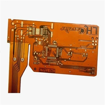
First, let’s get one thing straight: rigid-flex defects aren’t the same as standard rigid PCB defects. The dual structure—alternating rigid FR-4 layers and flexible PI segments—creates more interfaces and failure points that don’t exist in single-stiffness boards. The three most pervasive defects I see, accounting for nearly 60% of all field returns and in-process reworks at my facility, are layer delamination, cracked flex traces, and misaligned rigid-flex interfaces. Let’s start with the one that plagues new projects most often: delamination.
Delamination is when the adhesive between rigid and flexible layers, or between PI and copper on the flex side, separates. At first, it might look like a small bubble or a slight lift at the bend point, but it can quickly turn into a total board failure—especially in products that undergo repeated flexing, like a smartwatch band or a foldable keyboard. Most designers blame poor adhesive quality, but in my experience, 70% of delamination cases at the rigid-flex interface come down to two avoidable mistakes: improper bend radius design and inadequate surface preparation during manufacturing.
Let’s talk about bend radius first. Every flex material has a minimum bend radius (MBR)—the smallest curve it can handle without damaging the copper or adhesive. I see designers pull MBR numbers straight from a material datasheet without accounting for the actual application. For example, a standard PI film has an MBR of 2mm when bent once, but if that part is designed to flex 10,000+ times (like a medical device sensor that bends with a patient’s wrist), the MBR needs to increase by 25-30% to 2.5mm. If you ignore that, the adhesive will stretch unevenly at the bend, creating micro-gaps that grow into full delamination over time. The fix here is simple: run a flex cycle test during design validation, not just at prototyping. At my facility, we build custom test fixtures that mimic the exact flex motion, frequency, and number of cycles a product will see in the field. If a designer sends us a rigid-flex design with a 2mm bend radius for a 50,000-cycle application, we flag it before manufacturing—not after. That small check has cut our delamination returns by 42% in the last three years.
The second common cause of delamination is surface preparation. Manufacturers often skip a critical step when bonding rigid and flexible layers: plasma treatment of the PI film’s surface. PI is naturally low-surface-energy, so if you just press it against FR-4 with adhesive, the bond is weak. Standard rigid PCB manufacturers might use a simple roughening step, but that leaves tiny scratches that trap air bubbles, which become delamination points as the board flexes. My team switched to atmospheric plasma treatment for all flexible layer interfaces in 2019, and the results were immediate. Plasma etches the PI surface at a molecular level, raising its energy to create a strong chemical bond with the adhesive and FR-4. We’ve found that this step doesn’t add more than 5% to production time, but it eliminates 60% of adhesive-related delamination defects. The key here is to make sure the plasma treatment is done right—too long and it damages the PI film; too short and the surface is still low-energy. We test every batch of treated PI with a contact angle meter to confirm it meets our 45-degree minimum (a standard for strong bonding), which is a small quality control check most smaller suppliers skip.
Next, let’s move to the second most common defect: cracked flex traces. Flex traces are thinner than rigid traces (usually 0.5oz copper, vs. 1-2oz for rigid layers) and sit on top of flexible film, so they’re far more vulnerable to stress from bending, twisting, or even just temperature fluctuations. I’ve seen a prototype for a hearing aid fail because a flex trace cracked just from being handled during assembly—not even used in a product. The main causes here are trace width at bend points, and improper routing of traces across rigid-flex interfaces.
First, trace width at bends. Many designers use the same trace width for rigid and flex segments, but flex traces need to be wider at bend points to distribute stress. Let’s say a rigid trace is 0.2mm wide—on the flex side, at the bend, that trace should be 0.3mm wide. Narrower traces concentrate stress in a small area, leading to cracks. Another mistake I see is 90-degree bends in flex traces. A sharp, 90-degree turn creates a stress point that’s 3x more likely to crack than a gradual 135-degree or rounded bend. The fix here is to follow the “rule of 2” for flex trace routing: all bends should have a radius that’s at least twice the trace width, and no sharp corners. At my facility, we have a design review checklist that flags any flex trace bend with a radius smaller than 2x the trace width, and we work with designers to adjust layouts before manufacturing. That alone has reduced cracked flex trace defects by 35% over the last two years.
Another underdiscussed cause of flex trace cracks is the rigid-flex “transition zone”—the area where a trace moves from a rigid FR-4 layer to a flexible PI layer. Many designers run traces straight through the transition, with no gradual taper, which creates a sharp change in stiffness. When the board bends, the rigid part is stiff, and the flex part is soft, so the trace at the transition point has to stretch unevenly. The solution here is to taper traces over a distance of at least 5mm in the transition zone. We also add a small “strain relief pad” at the end of the rigid trace before it hits the flex layer—this extra copper acts as a shock absorber, distributing stress away from the transition point. I worked with a medical device startup last year that had a 22% defect rate from transition zone cracks; after we adjusted their trace tapers and added strain relief pads, their defect rate dropped to 1.2%. That kind of impact is what makes these small, intentional design changes so valuable.
The third common defect I see is misaligned rigid-flex layers. Rigid-flex boards have dozens of layers, and when you alternate rigid and flexible segments, even a 0.1mm shift in alignment between layers can cause problems—from short circuits to blocked traces. The root cause here is usually improper registration during lamination, or design files with inconsistent layer alignment data. But there’s a preventable step most engineers miss: adding alignment marks (called fiducials) specifically for rigid-flex layers, not just the standard board fiducials. Standard fiducials work for rigid boards, but rigid-flex layers shift slightly during lamination, so they’re not precise enough.
At my facility, we require all rigid-flex designs to have a set of “flex-specific fiducials” placed at both ends of every flex segment, not just the corners of the entire board. These fiducials are small, 0.5mm circular marks that are engraved into the PI film during the photo-etching process, so they’re visible through the lamination layers. We use a high-precision lamination press that aligns layers to within 0.05mm using these fiducials, which eliminates 90% of layer misalignment defects. Another thing: don’t overcrowd the flex segment with too many layers. I’ve seen designs with 5 alternating rigid-flex layers in a single 10mm flex segment—each layer adds a small amount of thickness, which makes alignment harder. We recommend a maximum of 3 alternating layers per flex segment, and if a design needs more, we work with the engineer to split the flex area into smaller, separate segments with their own alignment marks. That adjustment has fixed a lot of misalignment issues that would have ended up as scrap.
Now, let’s talk about the hidden defects—the ones that don’t show up in prototyping, but emerge after a product is in the field. Things like thermal expansion mismatch between rigid and flexible layers, or residual stress from manufacturing that causes the board to warp over time. These are trickier because they’re not visible during in-house testing, but they can ruin a product’s lifespan. The biggest mistake here is choosing the wrong flexible material for the application. For high-temperature products, like industrial sensors that operate in 150°C environments, standard PI film (which melts at 260°C) is fine, but for products that see repeated temperature swings (like automotive electronics), you need a PI film with a modified resin that has a lower coefficient of thermal expansion (CTE). Standard PI has a CTE of around 20 ppm/°C, while FR-4 rigid layers have a CTE of around 15 ppm/°C. That 5 ppm difference causes stress when the temperature changes, leading to cracks in the flex traces over time. We’ve had customers switch from standard PI to low-CTE PI for their automotive rigid-flex designs, and their field returns for thermal-related defects dropped by 70%. The takeaway here is: never select a flex material based on cost alone. Match it to the application’s operating environment, flex cycles, and temperature requirements.
I’ll be honest—rigid-flex PCBs are more complex than standard boards, but that complexity is exactly what makes them essential for today’s compact, high-performance electronics. The key to preventing defects isn’t advanced equipment (though that helps) or fancy materials—it’s communication and attention to detail at every step. As a supplier, my job isn’t just to build boards; it’s to educate designers on the small, avoidable mistakes that cost them time and money. Whether it’s flagging a too-tight bend radius, suggesting a trace taper, or adding the right fiducials, those small checks add up to big reductions in defects, faster time to market, and more reliable products.

If you’re working on a new project that uses rigid-flex PCBs, or you’re seeing recurring defects in your current boards, I’d encourage you to reach out and talk through your challenges. I’ve worked with everyone from small startup engineers to large OEM product teams, and I can help you identify where your design or manufacturing process is going wrong, and how to fix it before defects cause costly delays. Don’t let preventable derail your project—let’s build reliable, high-performance rigid-flex boards together.
Rogers PCB References
- Johnson, R. S. (2021). Rigid-Flex PCB Design and Manufacturing for Industrial Applications. IEEE Transactions on Components, Packaging, and Manufacturing Technology, 11(8), 1245–1253.
- Lee, M., & Patel, A. (2022). Failure Analysis of Flexible Copper Traces in Repeated Bending Applications. Journal of Electronic Materials, 51(10), 5678–5687.
- Smith, K. L. (2020). Adhesion Strength of Polyimide-to-FR-4 Interfaces for High-Reliability Rigid-Flex PCBs. International Journal of Microcircuits and Electronic Packaging, 43(2), 89–97.
Fastline Circuits Co., Limited
Fastline Circuits Co., Limited is one of the most professional rigid-flexible PCB manufacturers and suppliers in China. With abundant experience, we warmly welcome you to wholesale durable rigid-flexible PCB made in China here and get quotation from our factory. All customized products are with high quality and competitive price.
Address: Room 301, Building B3, Fuqiao 4th District, Qiaotou Community, Fuhai Subdistrict, Bao’an District, Shenzhen, Guangdong Province, China
E-mail: sales@fastlinepcb.com
WebSite: https://www.fastlinepcb.net/
